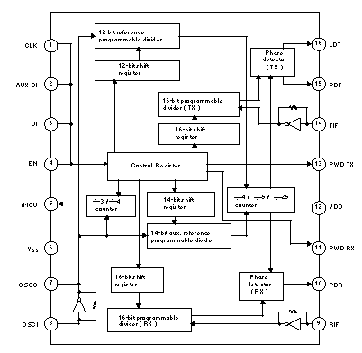

| Pin | Name | Description |
|---|---|---|
| 1 | CLK | Clock from CPU |
| 2 | AUX DI | |
| 3 | Data | Data from CPU |
| 4 | ST | Strobe from CPU |
| 5 | fMCU | Clock output terminal. This output pin provides the clock source for Micom or other system as an output of X - tal OSC ü 3 / ü 4. Which can be controlled by the bit of the control register. Clock output on / off control is possible by MICOM. |
| 6 | GND | Ground |
| 7 | RI | X-tal Oscillator Input |
| 8 | RO | X-tal Oscillator Output |
| 9 | RIF | á Input terminal of RX channel counter. á Usually, AC coupled output signal of VCO loop is introduced and the Minimum input signal level is 300mVp-p at 60 MHz |
| 10 | PDR |
á There are 3 - kind output signal states in PDR pin. - If fRX > fREF (fRX is leading), the output is negative pulse state - If fRX < fREF (fRX is lagging), the output is positive pulse state - If fRX = fREF (the same phase), the output is high impedance state |
| 11 | PWDRX | á This output terminal offers the state of internal RX channel counter operation. If this pin state is high, internal RX channel counter is operating in power saving mode. So, this pin can be used in appling the power switch on / off control. |
| 12 | VDD | Power supply input terminal |
| 13 | PWDTX | If this pin state is high, internal TX channel counter is operating in power saving mode. So, this pin can be used in appling the power switch on / off control. |
| 14 | TIF | á Usually, AC coupled output signal of VCO loop is introduced and the Minimum input signal level is 300mVp-p at 60 MHz |
| 15 | PDT | á There are 3 - kind output signal states in PDT pin. - If fTX > fREF (fTX is leading), the output is negative pulse state - If fTX < fREF (fTX is lagging), the output is positive pulse state |
This counter shows the number of hits since the 29th January 2000
Copyright © The Defpom 1997-2008